Blog
Window to the Nano World


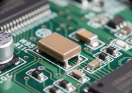
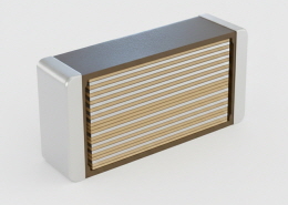
MLCCs (Multi-Layer Ceramic Capacitors) are essential passive components used in virtually all electronic devices, including smartphones, PCs, and automotive electronics. Built with stacked ceramic dielectric layers and metal electrodes, MLCCs are designed with extremely thin internal layers — often only a few micrometers or less than 1 μm thick.
To achieve higher capacitance, manufacturers continuously increase the number of layers while reducing their thickness. However, this process can introduce microcracks, voids, or delamination between layers, directly affecting product reliability and performance. Accurate observation of layer boundaries and internal defects is therefore critical for failure analysis and quality control, making SEM cross-section analysis an essential tool for MLCC evaluation.
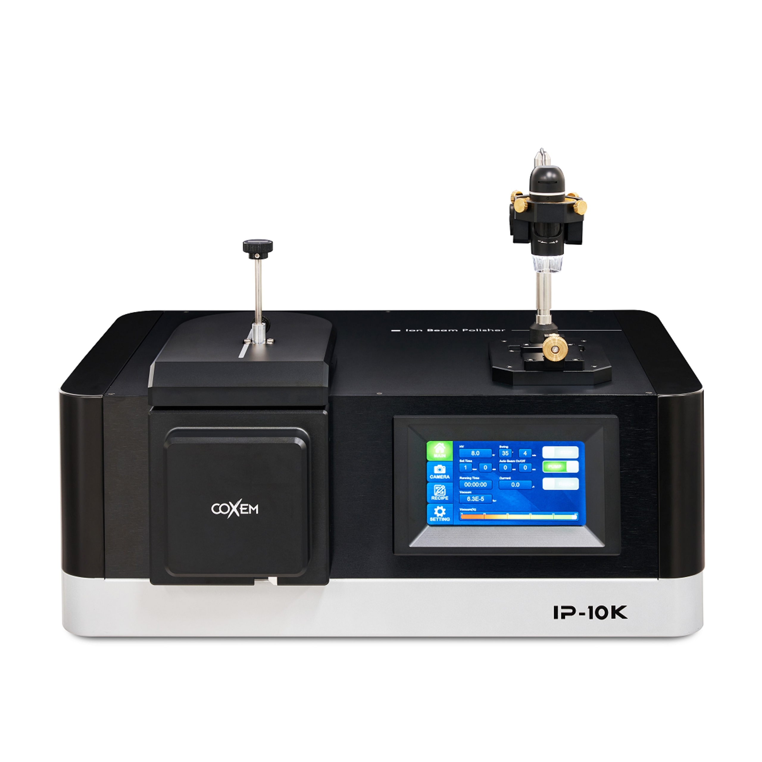
Creating a high-quality cross section without damaging these ultra-thin layers is especially important. Conventional mechanical polishing can cause structural deformation, smear fine features, or leave polishing residue that interferes with accurate analysis. In contrast, the COXEM IP-10K uses argon ion-beam milling to produce clean, damage-free cross sections with minimal physical or chemical artifacts.
For compact and highly detailed samples such as MLCCs, ion milling with the IP-10K followed by SEM imaging provides a highly effective solution for precise structural observation and defect analysis.
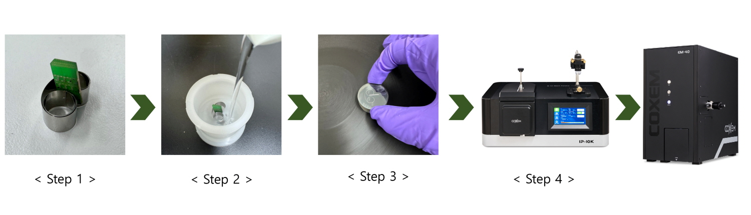
Due to the small size of MLCC samples, the specimen should first be embedded in resin before ion milling. Since heat can be generated where the ion beam interacts with the sample during milling, using a heat-resistant resin is recommended. For highly heat-sensitive samples, low-temperature curing epoxy and ion milling conditions below 5 kV are recommended to minimize thermal damage.
Step 1. Fix the sample vertically using a clip and place it into the mold.
Step 2. Mix the resin and hardener according to the recommended ratio, then pour the mixture into the mold.
Step 3. Cure the sample on a hot plate or at room temperature depending on the type of epoxy used.
Step 4. Remove the cured sample from the mold.
Step 5. Mechanically polish the sample to expose the target milling area.
Step 6. Mount the sample onto the IP-10K holder, perform ion milling, and observe the cross section using SEM.
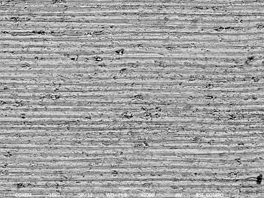
[MLCC, before ion milling]
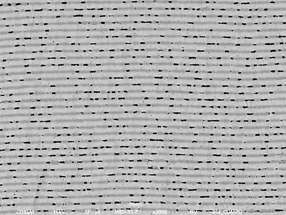
[MLCC, after ion milling]
이온 밀링 전의 시료를 SEM으로 관찰해보면 표면에 연마제에 의한 스크래치와 오염 물질이 남아있어 적층 구조가 제대로 보이지 않습니다. 이온 밀링 후에는 깔끔한 MLCC 단면을 얻어 내부 여러 층의 구조를 명확하게 관찰할 수 있었습니다.
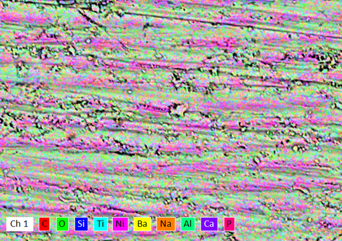
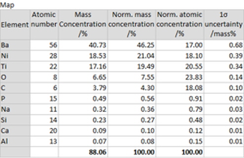
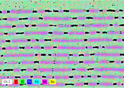
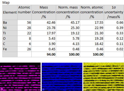
Elemental analysis was performed on the MLCC cross section before and after ion milling. Prior to ion milling, residual polishing compounds and surface contaminants remained on the sample, resulting in the detection of silicon from the polishing media along with other unwanted elements.
After ion milling, these contaminants were effectively removed, allowing only the intrinsic elements of the MLCC to be detected. The clean cross section also enabled clearer elemental distribution in the mapping images, providing more accurate and reliable analysis results.
#MLCC # SEM #EM-40 #Ionbeampolisher #IP-10K

 Trace Element Analysis with BEX