Blog
Window to the Nano World




Semiconductors are essential components used across industries including computers, smartphones, automotive electronics, and advanced industrial systems. They control and process electrical signals to deliver system functionality and performance. Depending on the application and operating environment, semiconductor devices are designed with highly sophisticated circuit structures, integration densities, and material compositions.
These devices contain densely integrated microstructures and fine patterns that are difficult to distinguish with the naked eye, enabling precise signal processing, power control, and data handling. As a result, semiconductors play a critical role in improving system performance, miniaturization, and long-term reliability across modern technologies.
Using SEM, semiconductor surfaces and internal microstructures can be observed at high resolution, allowing detailed analysis of fine pattern geometries, line width variations, interface defects, and contamination particles that are difficult to detect optically.
SEM is also highly effective for comparing structural changes before and after processing or reliability testing, helping identify the root causes of device degradation and failure. When combined with EDS, SEM can further analyze the composition and distribution of contaminants or dopant elements, making it a powerful tool for failure analysis, process optimization, material evaluation, and semiconductor reliability improvement.

The semiconductor sample surface is carefully flattened through step-by-step cutting and polishing processes to clearly expose interfaces between metal interconnect layers and insulating layers. During preparation, minimizing excessive mechanical stress and heat generation is important to prevent deformation of metal wiring and damage to dielectric materials.
The prepared sample is then securely mounted onto an SEM stub using carbon tape. Because semiconductor substrates often contain non-conductive materials, Au or Pt ion sputter coating is applied to reduce charge accumulation during SEM observation.
Step 1. Cut the sample to an appropriate size.
Step 2. Mount the prepared sample onto the SEM stub.
Step 3. Apply Au sputter coating using the SPT-20 to ensure stable SEM imaging.

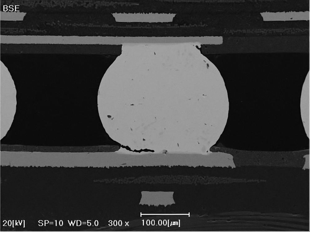
[Solder Ball]
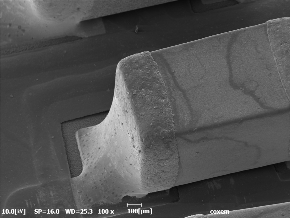
[PCB Mount]
Using the COXEM EM-30N, a PCB mounted with solder balls was observed by SEM at an accelerating voltage of 20 kV and a working distance of 5 mm using the SE detector.
The results showed that the solder balls maintained a relatively uniform spherical shape while being stably bonded onto the substrate pads. Continuous interfacial bonding structures between the solder balls and pads were also clearly observed. In addition, fine wiring patterns and pad structures on the PCB surface were visualized in detail.
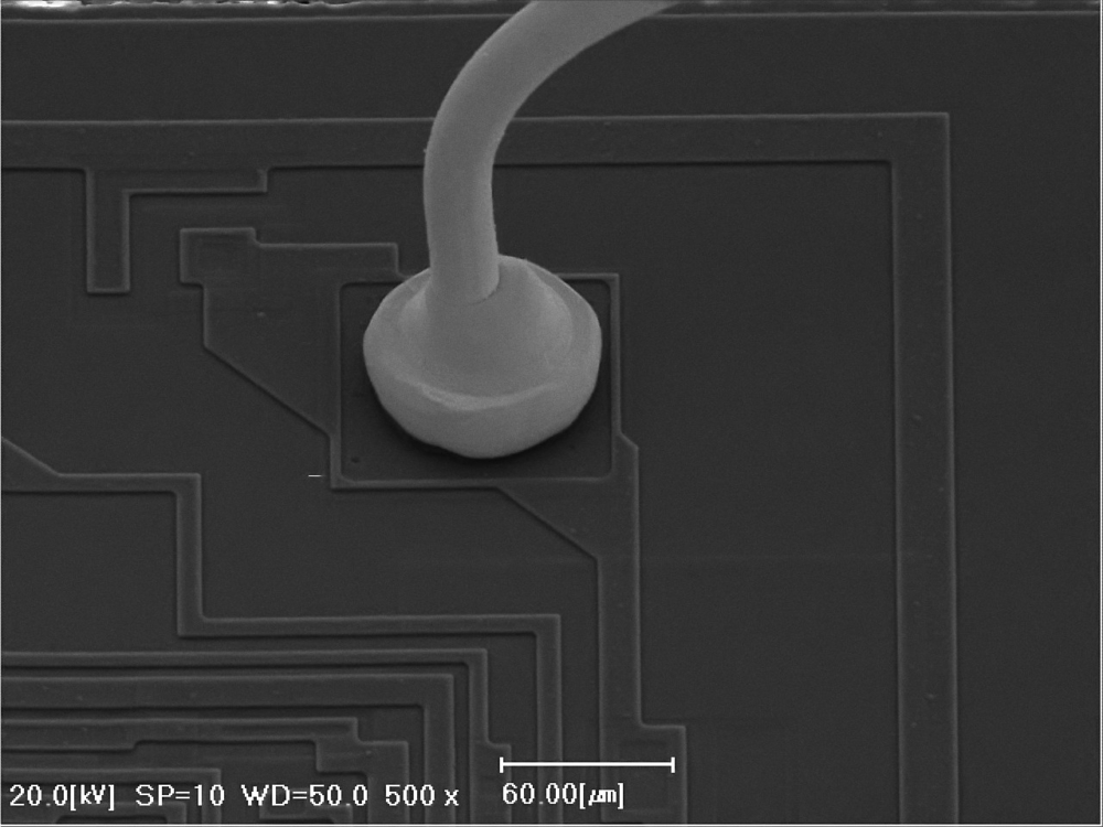
[Wire Bonding]
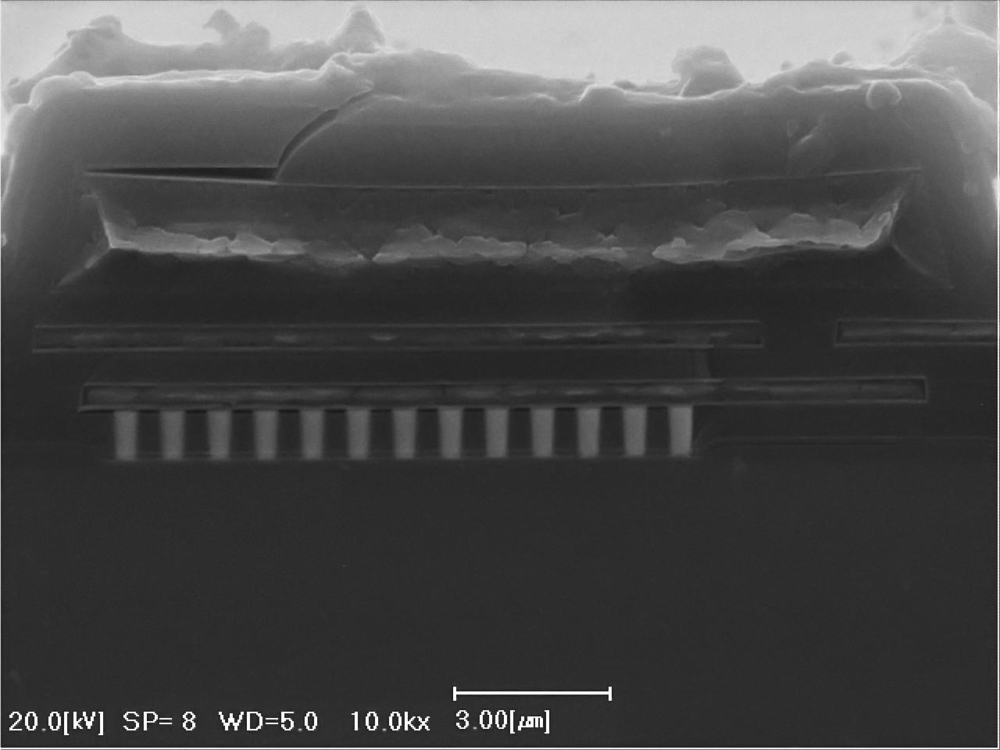
[PCB Cross Section]
Using the COXEM EM-30N, a semiconductor circuit board was observed by SEM at an accelerating voltage of 20 kV and a working distance of 8–13 mm using the SE detector.
The SEM images revealed repetitive pattern structures consisting of metal interconnects and insulating layers across the substrate surface. The spacing between interconnect lines and the line edge profiles appeared relatively uniform, indicating stable pattern formation. In addition, localized surface defects such as fine scratches and contamination particles were observed in certain regions, suggesting possible defects introduced during processing or handling.
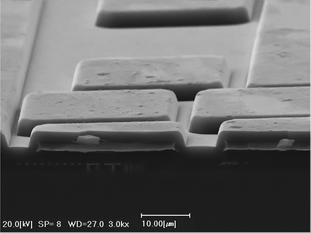
[PCB Cross Section]
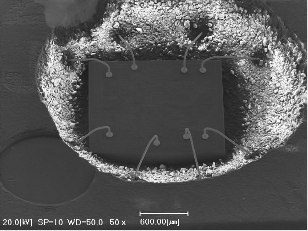
[Wire Bonding]
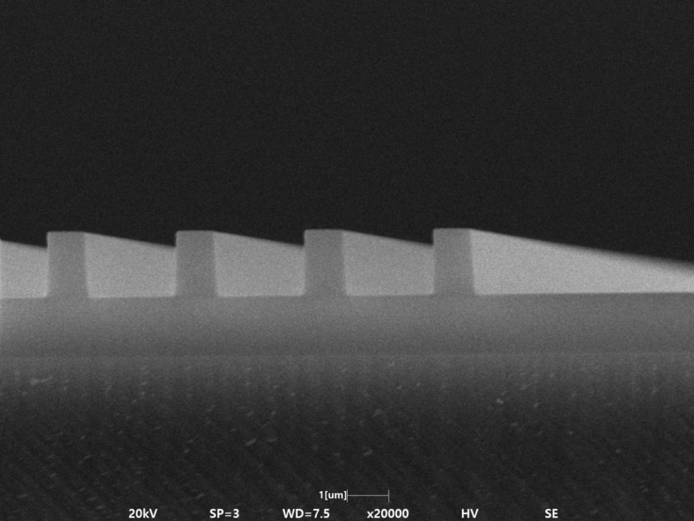
[Wafer substrate]

 Revealing the Hidden Structure of Human Hair with SEM