Blog
Window to the Nano World




Optical and phase-contrast microscopes are widely used for observing cellular morphology, but their structural limitations make it difficult to clearly distinguish fine surface features and internal density variations. In the bio industry, more advanced analytical tools are required for precise characterization of microscopic biological structures.
SEM provides an efficient and cost-effective solution by enabling both surface and internal analysis at high resolution within a single platform. Its versatile imaging capabilities allow researchers to investigate biological samples with greater structural detail and analytical flexibility.
The SE mode is optimized for high-resolution observation of fine surface morphology and texture. Stable surface imaging can typically be achieved with simple drying and minimal conductive coating.
The VP (Variable Pressure) mode offers additional advantages by maintaining a low-vacuum environment, helping minimize charging and beam-induced thermal damage. This makes VP imaging particularly suitable for heat-sensitive biological samples and non-conductive materials.
The EM-40 used in this analysis features a relatively compact chamber design, enabling more stable low-vacuum operation for biological sample observation.
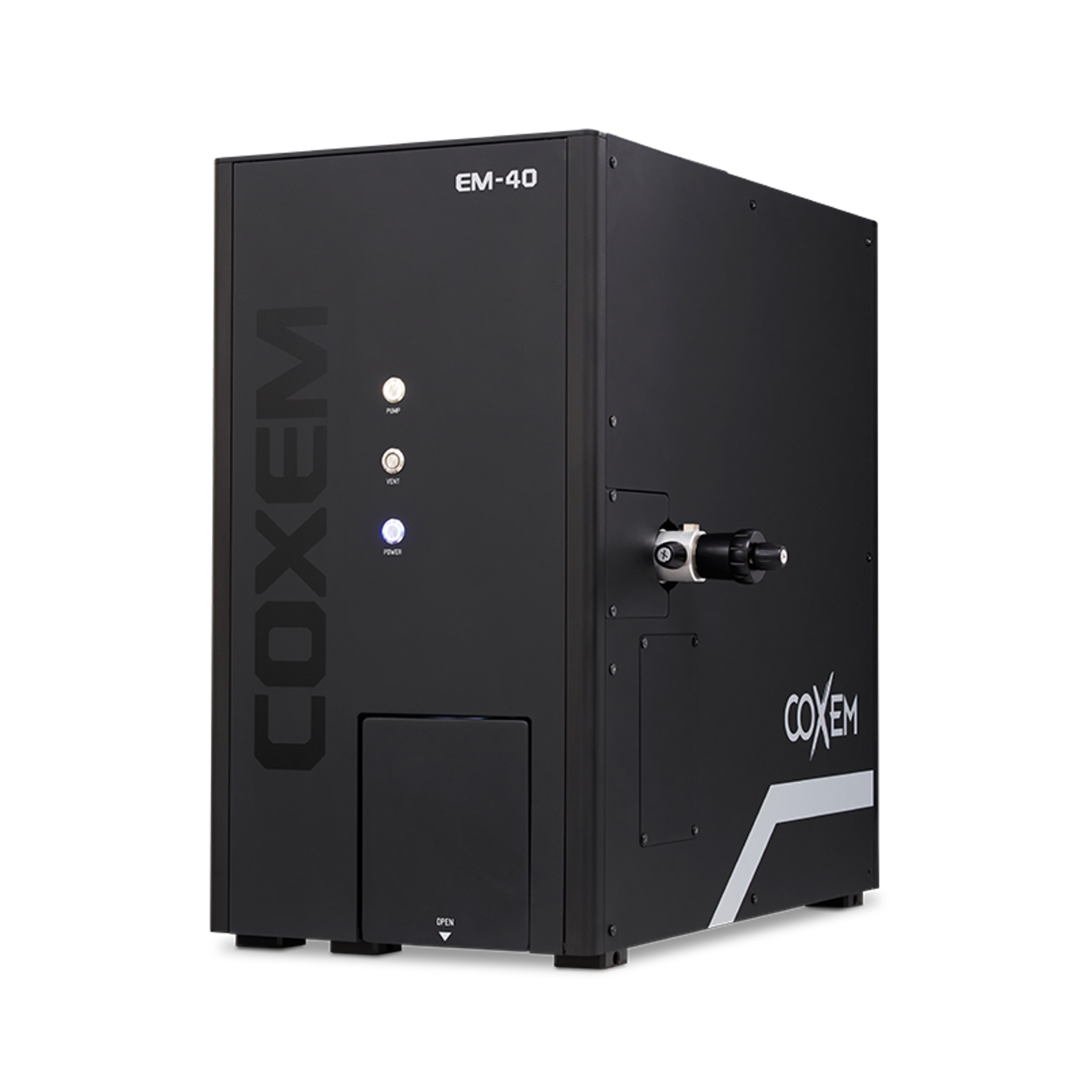
Biological samples can be easily damaged by physical impact during collection, so careful handling is essential to minimize structural deformation. Depending on the sample type, proper dilution may also be required to prevent particle agglomeration, which can interfere with accurate morphology observation in SE mode.
Conductive coating thickness should be carefully controlled. If the coating is too thin, image noise caused by charging effects may occur, while excessively thick coatings can obscure fine surface structures. A coating thickness of approximately 5–10 nm is generally recommended.
Step 1. Mount the collected sample onto the SEM stub using conductive tape.
Step 2. Apply conductive coating using the SPT-20 sputter coater.
1) Recommended coating condition: 3 μA, 300 s
2) Coating may be omitted when using VP mode
Step 3. Load the prepared sample into the SEM chamber and observe the surface morphology.


[Egg White]

[Lotus Leaf ]

[Plantain]

[Penicillium]
Scanning electron microscopy (SEM) is not limited to specific specimens or organisms, but can be broadly applied to a wide variety of biological and non-biological samples. For example, SEM can clearly visualize aggregated protein structures inside egg white at high resolution, while also capturing the detailed surface morphology of microscopic particles such as flower pollen.

[Fungal Hyphae]

[Insect Wing]

[Fish Fry]

[20kV]

[5kV]
This image of lactic acid bacteria was acquired using a low-voltage imaging mode, which effectively minimizes thermal damage caused by the electron beam. In addition, low-voltage operation helps suppress charging effects commonly observed in non-conductive samples, allowing finer surface structures to be observed more clearly and stably.
For these reasons, low-voltage SEM imaging is particularly useful for analyzing heat- and charge-sensitive biological specimens.

[HV]

[VP]
This image of a balloon flower root was acquired using VP (Variable Pressure) mode. Non-conductive samples typically require conductive coating before SEM observation, but VP mode effectively suppresses charging effects, enabling stable imaging even without coating.
By finely controlling the chamber vacuum level under low-vacuum conditions, VP mode can optimize imaging conditions according to the sample characteristics. This makes it especially useful for observing biological specimens or natural-state samples that are difficult to coat.

[Egg White, LV]

[Ant, VP]

[Paper, VP]

 Exploring the Microscopic World of Living Organisms with SEM