Blog
Window to the Nano World



Metal surfaces can be examined using optical microscopes or surface roughness testers, offering fast and convenient inspection of surface conditions. However, these methods have limitations in resolution and surface sensitivity. In contrast, SEM enables observation of fine microstructures at the nanometer scale, revealing detailed surface features with significantly greater clarity.
Thanks to its high depth of field, SEM also provides highly three-dimensional images, making it especially effective for analyzing micro-defects, surface damage, and early-stage failure sites on metal surfaces.
In this application, various metal samples will be analyzed using the CX-200K. Equipped with a precise 5-axis stage, the system allows accurate control of sample position and tilt, enabling optimized detector geometry and highly reproducible analysis conditions.
The structural design of the CX-200K is also well suited for EBSD applications, providing a stable and reliable analysis environment for metal samples with a wide range of shapes and sizes.

Metal samples generally do not require conductive coating because they are inherently conductive. However, thin conductive coating may still be applied to improve image quality and enhance EBSD analysis performance. To avoid masking fine surface features, a coating thickness of approximately 5–10 nm is recommended.
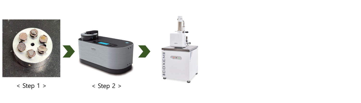
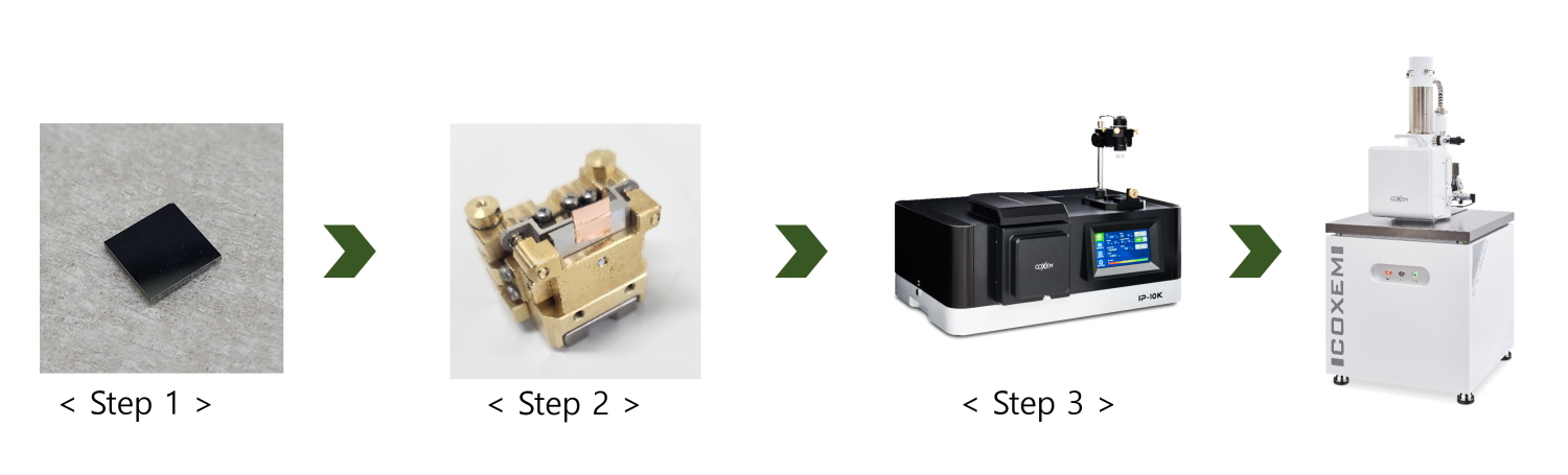
Step 1. Mount the collected sample onto the sample holder using conductive tape.
Step 2. Apply conductive coating using the SPT-20 sputter coater.
1) Coating condition: 3 μA, 300 s
Step 3. Load the coated sample into the SEM and observe the surface morphology.
[SE Image]
[BSE Image]
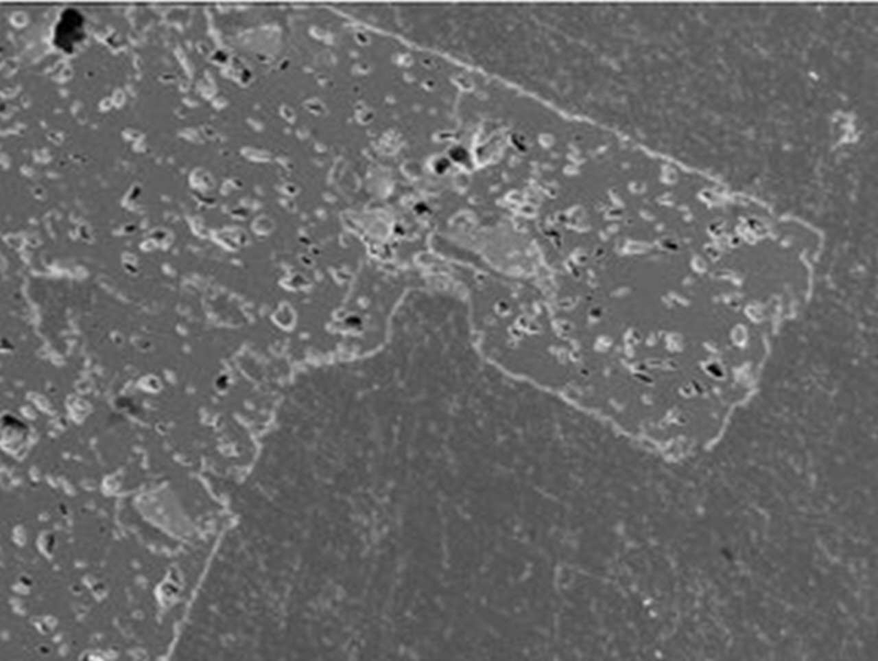
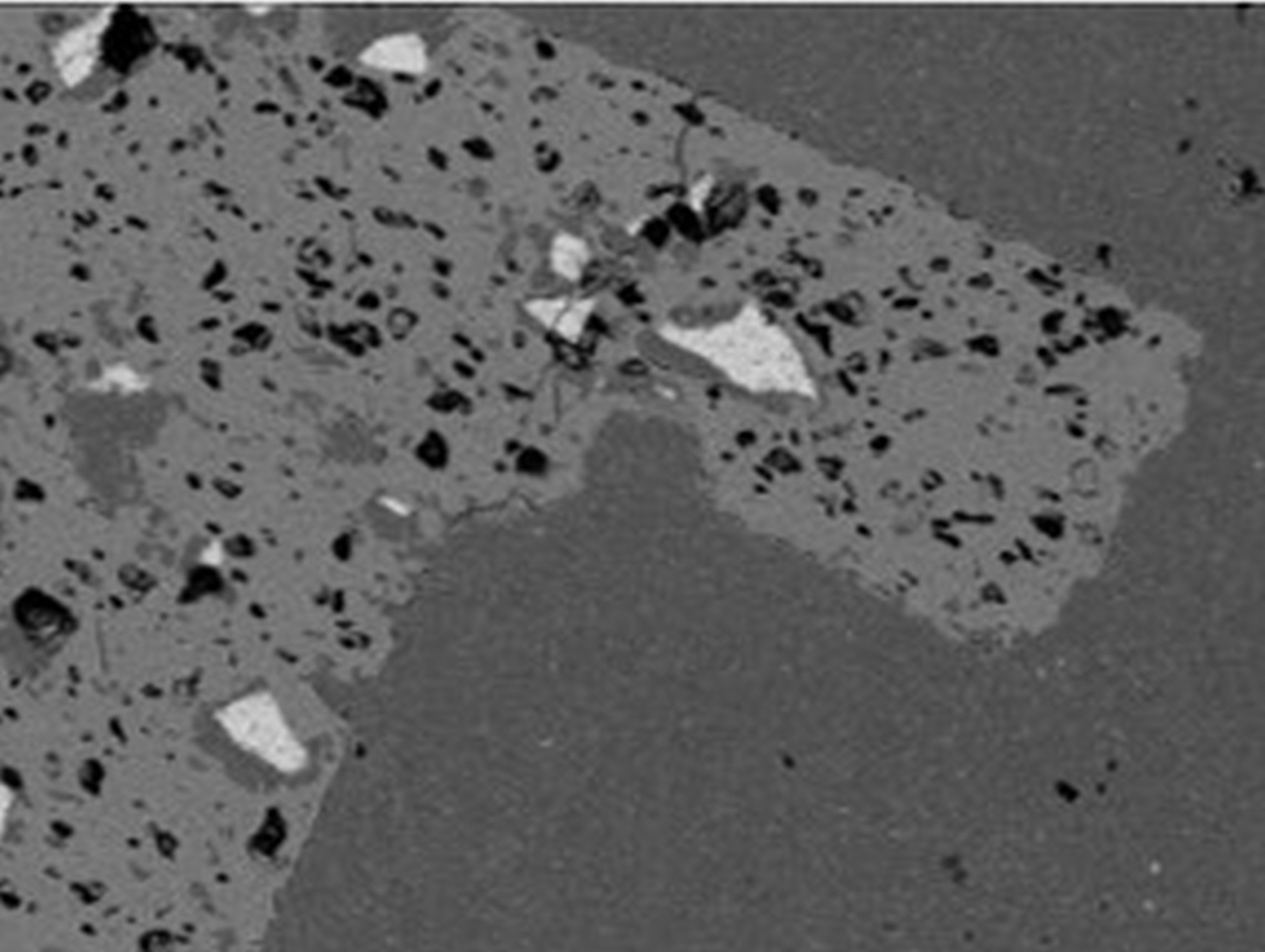
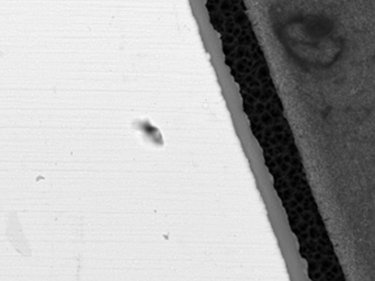
This image shows an alloy sample observed in BSE mode. Because BSE imaging utilizes signal intensity differences based on atomic number contrast, organic and inorganic particles can be clearly distinguished even without additional elemental analysis equipment.
This allows particle distribution and compositional differences within the sample to be visualized with strong contrast, making BSE imaging highly effective for material characterization and quality evaluation.
[BSE Image]
[Deep 3D Image]
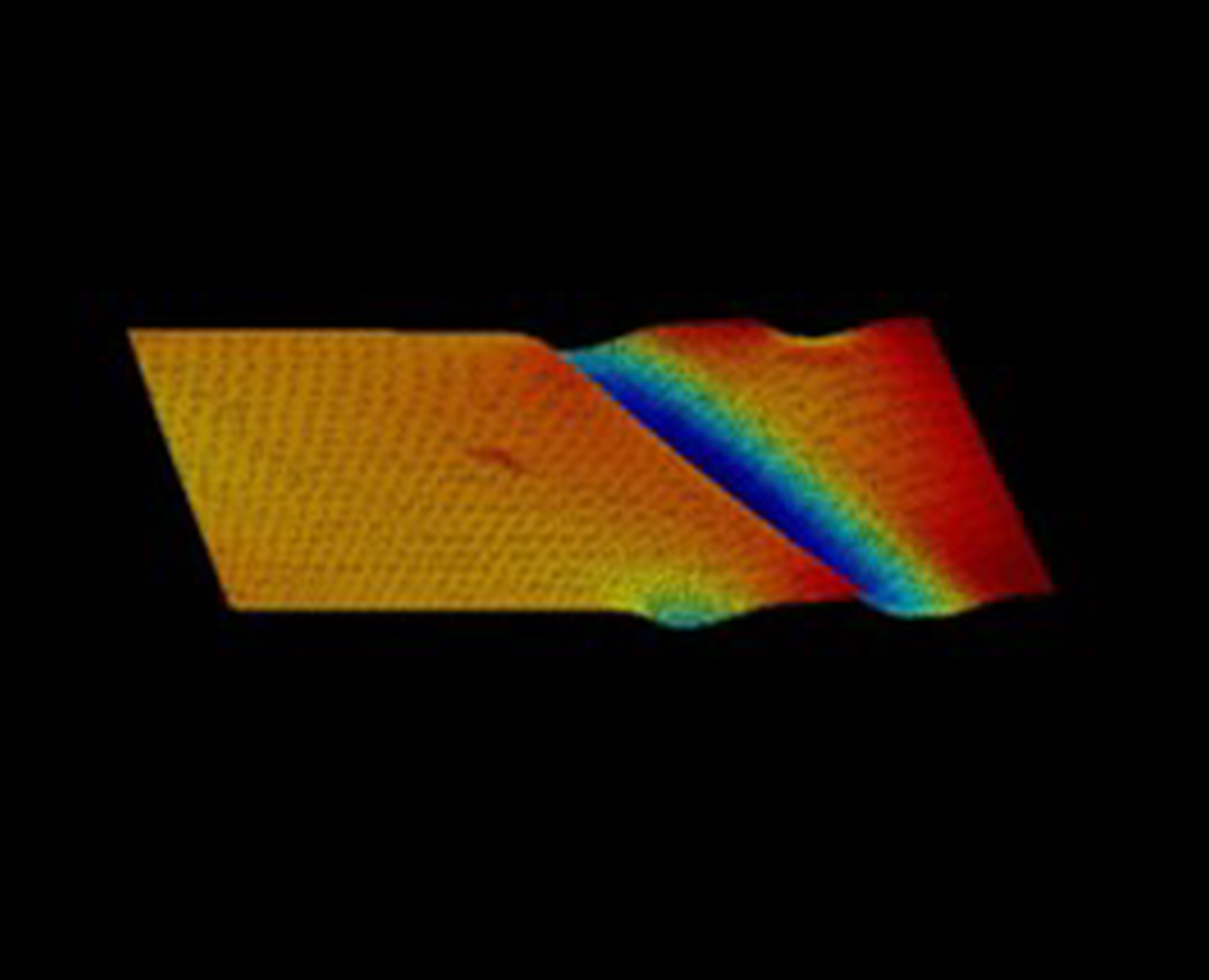
This image was acquired using Deep3D mode, enabling precise analysis of not only the sample morphology but also three-dimensional information such as height and spacing.
Higher regions are displayed in red while lower regions appear in blue, providing intuitive surface visualization. In addition, the profile graph below allows quantitative measurement of height differences across specific areas of the sample.

[Heat-treated Metal]
[Heat-treated Metal: BSE Image]

[Metal Wire: BSE Image]
Accurate EBSD analysis requires a well-polished sample surface capable of generating clear Kikuchi patterns. If the surface is insufficiently polished, reliable EBSD results cannot be obtained, making sample preparation one of the most critical steps in the EBSD workflow.
Step 1. Cut the sample to an appropriate size and mechanically polish the surface to minimize height differences.
Step 2. Perform fine surface polishing using an ion polisher to achieve a damage-free finish.
Step 3. Load the polished sample into the SEM for EBSD observation and analysis.
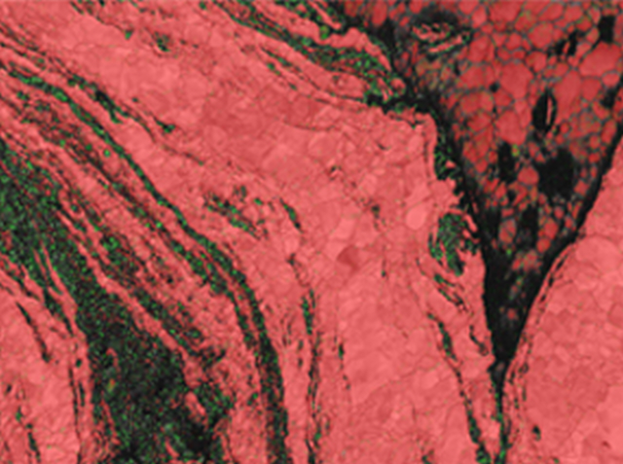
[EBSD : Phase Map]
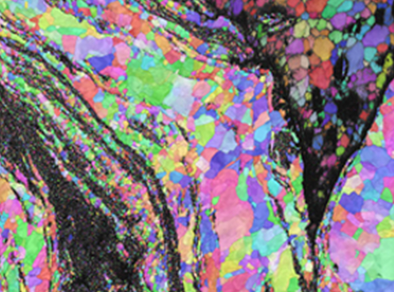
[EBSD : IPFX Map]
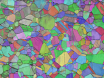
These images show EBSD analysis results of a copper alloy sample acquired using the EBSD system integrated with the EM-40. EBSD supports various filtering and mapping options depending on the analysis objective, allowing specific structural and crystallographic information to be effectively highlighted.
The image on the left is a Phase Map used to distinguish different crystal phases, while the image on the right is an IPFX Map showing crystal orientation relative to the X-axis direction of the sample.
[Cu-Ni Alloy ]
[Fe BCC MO average]
[Cu-Fe Alloy IPFX Map ]

 Uncovering Hidden Microstructures in Rocks with SEM