Blog
Window to the Nano World


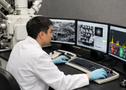

Large Area Analysis enables comprehensive inspection of defects such as microcracks, contamination, coating non-uniformity, and particle distribution across an entire sample area. Unlike localized observation, wide-area SEM analysis helps identify defects that may otherwise be overlooked, providing a more accurate understanding of overall sample conditions.
Its high reproducibility and excellent documentation capability also make large-area analysis highly valuable for research, quality assurance (QA/QC), defect tracking, process optimization, and production stability across a wide range of industries.
SEM-based Large Area Analysis has become an essential tool for quality control and failure investigation in modern industries. SEM enables high-resolution observation of fine particles, surface structures, and defects that are difficult to detect using optical microscopy alone, allowing more accurate evaluation of particle origin and morphology.
When combined with EDS, SEM can also provide rapid elemental analysis for identifying contaminants and tracing sources of process abnormalities, product defects, or foreign materials. These advantages make SEM Large Area Analysis widely used in semiconductor, battery, automotive, environmental, and advanced manufacturing applications where product reliability and process stability are critical.
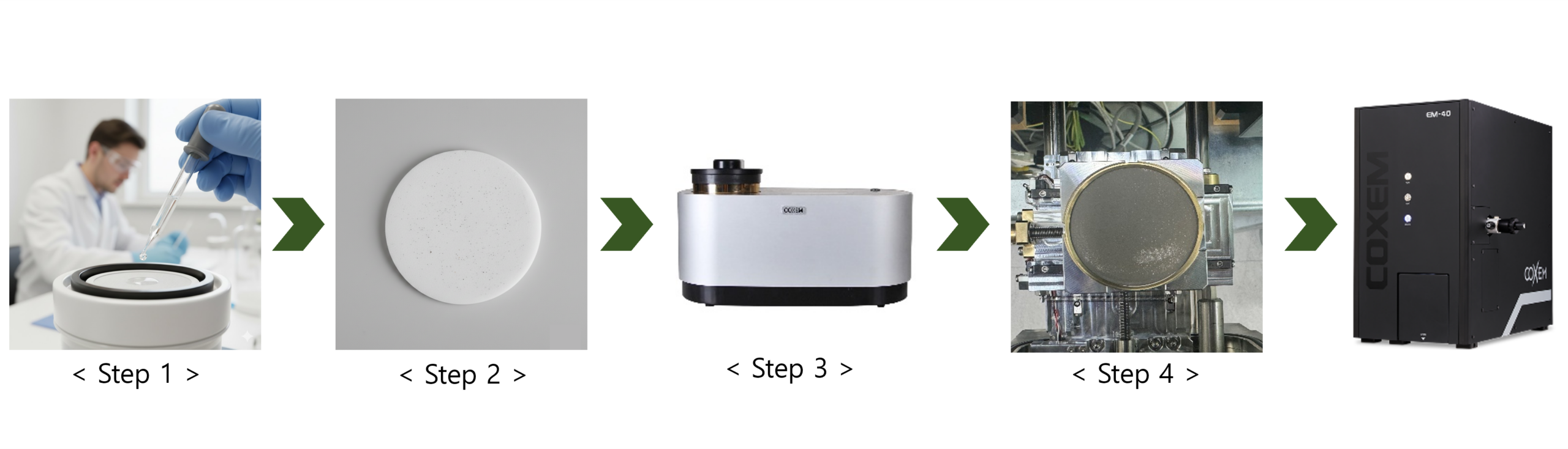
The sample is first diluted and dispersed in a solvent such as distilled water or ethanol to ensure uniform particle distribution without aggregation. The dispersed solution is then deposited onto the filter surface.
After deposition, the filter is completely dried at room temperature or under low-temperature drying conditions to remove moisture while minimizing filter deformation. The dried filter is mounted flat onto an SEM stub using carbon tape or silver paste, starting from the edges to maintain surface uniformity.
To improve conductivity, a thin Pt or Au coating is applied using an ion sputter coater such as the SPT-20. This preparation enables stable large-area SEM imaging and particle distribution analysis across the entire filter surface.
If necessary, marking the edge of the filter can also improve positional reproducibility during panorama imaging or mapping analysis.
Step 1. Dilute the sample in a solvent and uniformly disperse it onto the filter surface.
Step 2. Completely dry the filter at room temperature or under low-temperature conditions to minimize deformation.
Step 3. Apply Au sputter coating using the SPT-20 to ensure surface conductivity.
Step 4. Apply Au sputter coating using the SPT-20 to ensure surface conductivity.

[Microplastic]
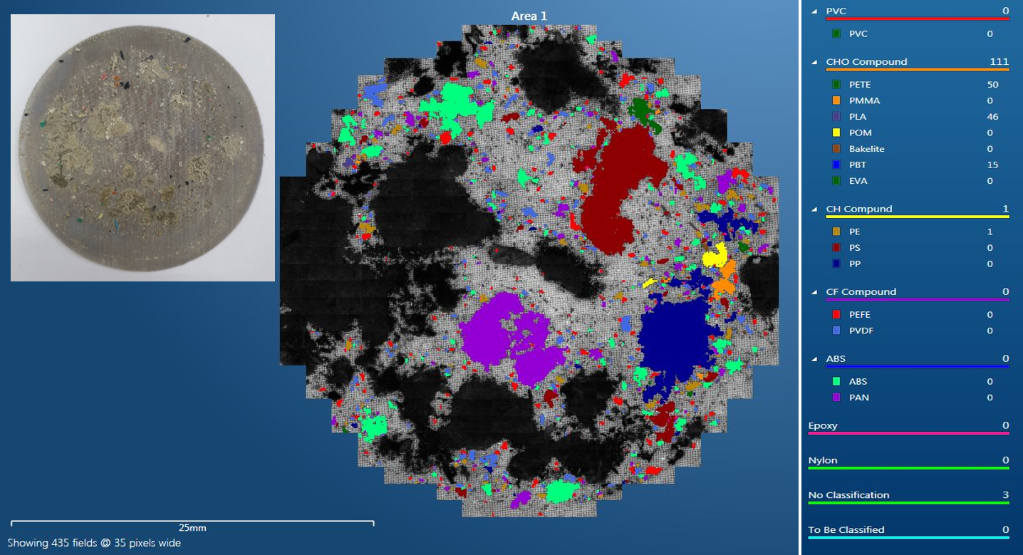
[Particle Analysis of Microplastic-Containing Membrane Filters]
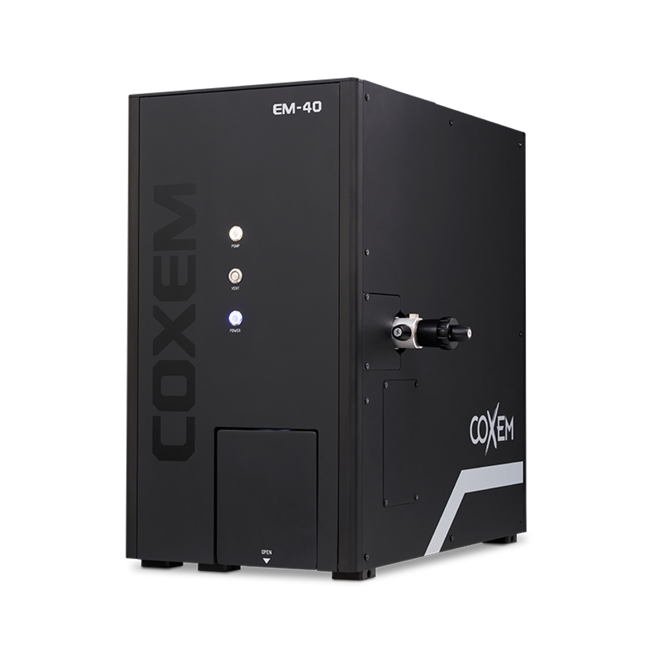
COXEM’s EM-40PE tabletop SEM is optimized for particle analysis, enabling high-resolution observation of the morphology, size, and surface characteristics of microplastics. In addition, EDS analysis allows identification of elemental composition — such as carbon, oxygen, and additive-related elements — helping trace plastic types and contamination sources.
With minimal sample preparation and fast analysis workflow, the EM-40PE provides an effective solution for environmental monitoring and industrial contamination analysis.

[Au Target]

[Large Area Mapping Analysis of Fine Particles on an Au Target]
COXEM’s Large Area Mapping function enables fast, high-resolution scanning of wide areas such as 45 mm membrane filters, allowing particle distribution, density, and morphology to be evaluated at a glance.
With automated panorama mapping, large sample areas can be seamlessly stitched into a single integrated image, improving the accuracy of quantitative analysis and process monitoring. This makes it a powerful solution for high-throughput sample inspection and contamination tracking in industrial environments.
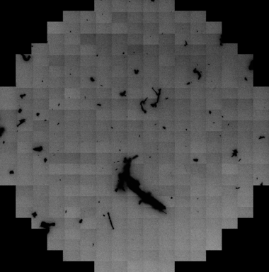
[Fine Particles on an Au Target]
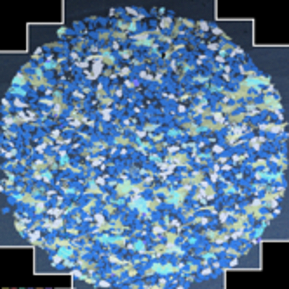
[Geological Material]

[Dust]

 Exploring Leaf Surface Structures with SEM