Blog
Window to the Nano World


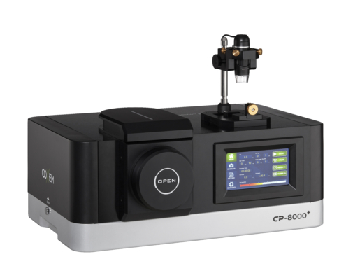

Fig CP-8000+ Ion Beam Polisher and EM-30N Tabletop SEM provided by COXEM Co.,ltd
In advanced semiconductor packaging such as Ball Grid Array (BGA) components, precise analysis of solder ball interiors and joint quality is critical for ensuring product reliability and improving yield. However, traditional mechanical polishing methods often cause mechanical stress or deformation, which can compromise the accuracy of the analysis.
To overcome these limitations, COXEM offers an integrated solution that combines the CP-8000+ Ion Beam Polisher and the EM-30N Tabletop Scanning Electron Microscope (SEM), enabling distortion-free surface preparation and high-resolution imaging.
The CP-8000+ uses high-energy argon ion beams to gently mill the sample surface in a completely non-contact manner. This eliminates mechanical damage and ensures an ultra-smooth and flat cross-section. It is ideal for preparing both vertical and curved surfaces, which are commonly found in advanced semiconductor packages.
Once the sample is prepared with the CP-8000+, the EM-30N provides high-resolution imaging at magnifications ranging from x130 to x500. With flexible observation modes such as SE (Secondary Electron) and BSE (Backscattered Electron), a wide range of surface and internal information can be obtained. An optional EDS (Energy Dispersive Spectroscopy) module enables further elemental analysis.
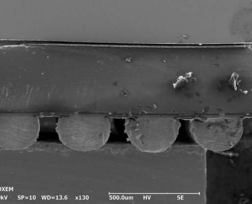
Fig SEM Images Before Ion Milling
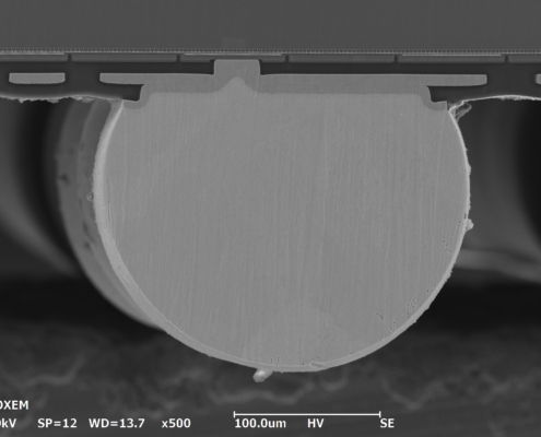
Fig SEM Images of Cross-Sectioned Sample with SE Image
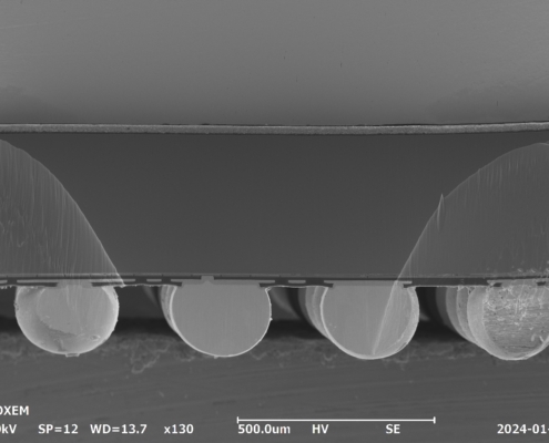
Fig SEM Images After Ion Milling
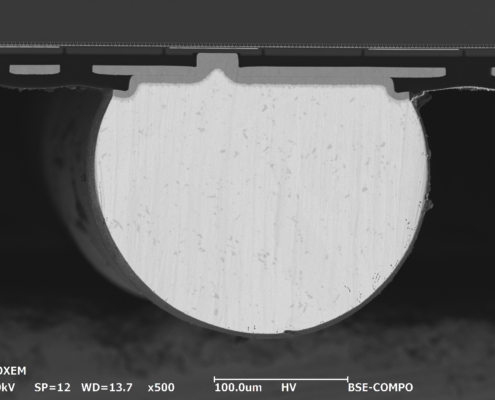
Fig SEM Images of Cross-Sectioned Sample with BSE Image
| Item | Traditional Mechanical Polishing | CP-8000+ Ion Beam Polishing |
| Surface Quality | Rough and uneven | Smooth and flat |
| Structural Clarity | Difficult to distinguish internal features | Clear identification of interfaces and defects |
| Risk of Damage | Mechanical stress and potential damage | No damage due to non-contact processing |
| Equipment | Key Features |
| CP-8000+ | High-energy ion milling, damage-free cross-sectioning, precision surface prep |
| EM-30N | 5 nm resolution, multiple detector options, intuitive user interface |
| Applications | Semiconductor packaging, electronics, materials analysis, failure investigation |
Conclusion: Your Ideal Solution for Reliable Cross-Section Analysis
Accurate cross-section analysis is essential for process optimization, defect identification, and overall yield improvement. COXEM’s integrated workflow, using the CP-8000+ and EM-30N, streamlines the process from surface preparation to high-resolution imaging, ensuring faster, more reliable, and repeatable results.
For industries requiring detailed and reproducible analysis—especially in semiconductor and electronic packaging—this solution sets a new benchmark for quality and efficiency.
#TabletopSEM #EM-40 #Ionbeampolisher #IP-10K #Crosssection

 Sunblock