Blog
Window to the Nano World


The semiconductor industry manufactures core components essential for electronic devices and computer systems, forming the foundation of modern technology and playing a critical role in global industrial and technological advancement. Major semiconductor products include integrated circuits (ICs), memory chips such as DRAM and NAND, and processors including CPUs and GPUs.
Semiconductor chips consist of billions of transistors and circuit structures densely integrated into extremely small areas. For stable device performance, each component must be precisely fabricated and accurately interconnected. Due to the microscopic scale and structural complexity of semiconductor devices, minimizing defects through highly controlled manufacturing processes is essential.
By preparing semiconductor surfaces or cross sections through ion milling and observing them with SEM, defect depth and failure locations can be accurately identified, enabling detailed root-cause analysis and process optimization.
COXEM’s IP-10K is an argon ion-beam polishing system designed for precise cross-section and surface preparation. Using argon ion milling, the system produces clean, damage-minimized surfaces for high-quality SEM observation. Because argon is chemically inert, the process minimizes unwanted chemical reactions, allowing more reliable compositional and structural analysis of semiconductor materials.

For large-area flat milling, the sample is first embedded in epoxy and mechanically polished to expose a uniform milling surface. Since flat milling removes only a fine surface layer, excessive surface roughness can significantly reduce milling effectiveness.
COXEM recommends preparing the sample surface to a roughness below 1 μm prior to flat milling for optimal polishing results.
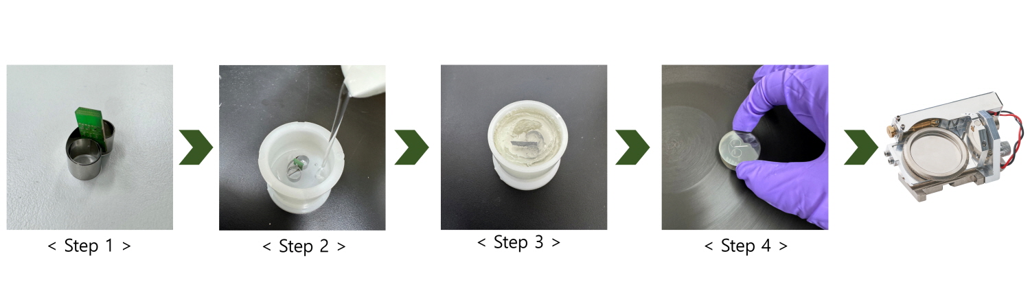
Step 1. Cut the sample to an appropriate size and secure it in a clip so it fits inside the mold.
Step 2. Mix the cold-mounting resin and hardener according to the recommended ratio.
Step 3. Place the sample into the mold and pour the mixed epoxy into the mold.
Step 4. Allow the epoxy to fully cure at room temperature, then remove the hardened sample from the mold.
Step 5. Perform mechanical polishing from coarse to fine polishing stages until the final surface roughness is below 1 μm.
Step 6. After polishing, mount the sample onto the flat milling holder for ion milling.

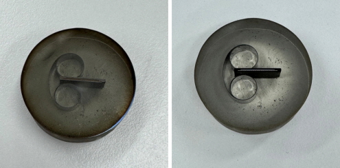
[Flat Milling Holder Mounted on the IP-10K]
[Before and After ion Milling]
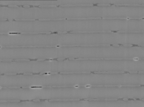
Flat milling was performed for 10 minutes using a 4 kV ion beam at an incident angle of 88°. Before ion milling, coating residues and surface contaminants on the molded sample interfered with clear SEM observation. After milling, the surface was cleanly polished, revealing the underlying structure with significantly improved clarity.
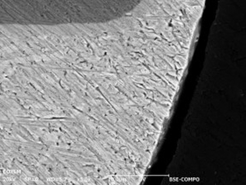
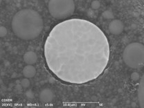
[Solder Ball, Before Milling]
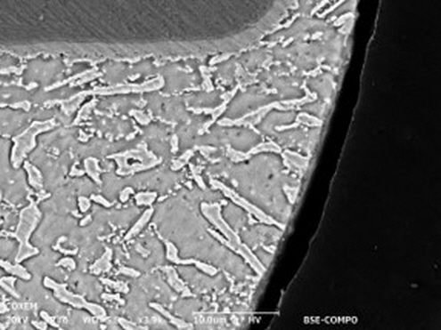
[Solder Ball, After Milling]
The same region of the sample was compared before and after ion milling. Prior to ion milling, scratches from mechanical polishing and residual polishing contaminants remained on the surface, making it difficult to clearly observe the solder ball cross section.
After ion-beam milling, surface contaminants and polishing scratches were effectively removed, allowing the internal particle boundaries within the solder ball to be observed much more clearly.
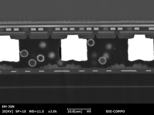
[chip]
[solder ball]
[MLCC]
 Eggshell Membrane